
#2-VLSI Design Flow Explained (with a DFT Perspective)
A Step-by-Step Walkthrough of the Chip Design Process with DFT Checkpoints

If you're entering the world of VLSI, understanding the full chip design lifecycle is non-negotiable.
In this issue of “VLSI by Ankit” newsletter series, I’m breaking down the VLSI Design Flow—highlighting key stages and where DFT (Design for Test) fits in. Whether you're a student, a fresher, or someone pivoting into hardware design, this is your foundation.
Think of VLSI like building a city — every stage is like laying the blueprint, building infrastructure, optimizing utilities, and finally handing over the keys.
VLSI Design Flow: Step by Step
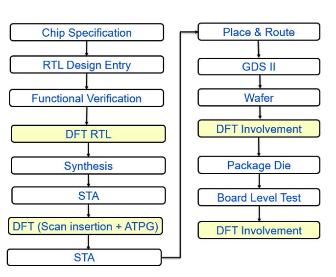
Front-End Flow:
Chip Specification
Everything starts here: architecture, features, performance goals, and test requirements are documented.RTL Design Entry
The chip’s functionality is described in RTL (typically Verilog or VHDL).Functional Verification
Ensure the RTL design behaves as expected using simulation and testbenches.DFT RTL
Add DFT structures early in the RTL itself. This could include test points, scan enable signals, etc.Synthesis
Convert the RTL into a gate-level netlist using synthesis tools like Design Compiler or Genus.Static Timing Analysis (STA)
Verify the timing of the design across various corners and constraints.Scan Insertion + ATPG
Add scan chains and generate automatic test patterns using tools like DFT Compiler or Tessent.
Back-End Flow:
Place & Route
Physical implementation—place standard cells, insert clocks, and route connections.GDSII Generation
Final layout data sent for fabrication.Wafer Fabrication
The silicon wafer is manufactured.DFT Involvement
Post-silicon validation, wafer-level test using the ATPG patterns.Package Die & Board Level Test
The chip is packaged and tested again on the board.DFT Involvement
Final tests to catch board-level or package-level defects.
Where Do Different Roles Fit In ?
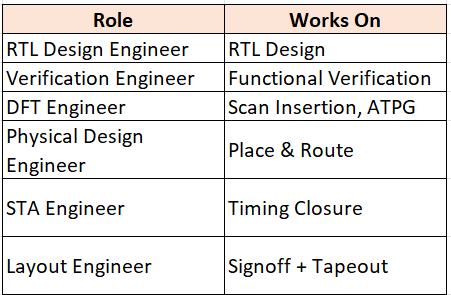
Each engineer works at a specific level of the flow, but all stages must sync perfectly.
Why DFT Matters So Much ?
DFT engineers work across RTL, synthesis, and post-silicon stages. Without well-inserted scan chains and good ATPG patterns, chips might pass design checks but fail in the field.
This cross-stage involvement makes DFT a critical, underrated part of the design cycle.
I regularly share VLSI insights, industry updates, and career tips.
🔗 LinkedIn: Kumar Ankit